


LED packaging refers to the process of enclosing LED chips within a protective package or module that provides electrical connections, thermal management, and optical functionality. The development status and trends in LED packaging involve advancements in packaging structures, manufacturing processes, and emerging technologies. Here’s an overview.
Surface Mount Device (SMD):
SMD packages are widely used in LED displays and lighting applications. They have a flat bottom surface and leads for surface mounting onto circuit boards, enabling high-density packaging and automated assembly.
Chip Scale Package (CSP):
CSPs have a smaller form factor as they eliminate the need for traditional packaging substrates. The LED chip is directly mounted onto a substrate, reducing package size and improving thermal performance.
Flip Chip:
In flip chip packaging, the LED chip is inverted and directly bonded to the package substrate, allowing for improved electrical and thermal performance. Flip chip packaging enables high-power and high-density LED applications.
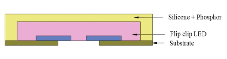
LED package-flip clip LED
Wire Bonding:
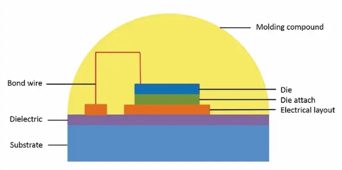
Wire bonding is a common method used to connect the LED chip to the package or substrate using fine metal wires (such as gold, aluminum, or copper). It provides electrical connectivity and mechanical support.
Die Attach:
The LED chip is affixed to the package or substrate using die attach materials, such as epoxy or solder. This process ensures proper alignment and thermal conduction between the chip and the package.
Encapsulation:
Encapsulation involves applying a protective layer (epoxy or silicone) over the LED chip to protect it from environmental factors, enhance light extraction, and improve reliability.
Miniaturization:
LED packaging is moving towards smaller form factors, such as CSP and miniaturized SMD packages, to enable compact and lightweight LED devices.
High-Power Packaging:
With the demand for high-power LEDs, packaging techniques are evolving to handle increased thermal management requirements and improve efficiency.
Advanced Thermal Solutions:
To enhance heat dissipation, new packaging structures incorporate advanced thermal management materials, such as ceramic substrates and metal-core printed circuit boards (MCPCBs).
Chip-on-Board (COB):
COB technology involves directly mounting LED chips onto a substrate, providing high lumen output, improved color mixing, and uniform illumination for applications like LED lighting modules.
Wafer Level Packaging (WLP):
WLP integrates the packaging process into the wafer fabrication steps, reducing costs and enabling high-volume production. It offers benefits like smaller form factors and improved electrical performance.
These trends aim to improve LED performance, efficiency, reliability, and cost-effectiveness while addressing the demands of various applications, including displays, lighting, automotive, and more. Continued advancements in packaging structures, materials, and processes contribute to the evolution of LED technology.