


The performance of an LED display depends on more than just the LED chip itself — it’s also about how that chip is packaged. Over the past two decades, LED packaging technology has evolved from traditional wire bonding to advanced flip-chip and COB (Chip on Board) structures. Each leap has delivered improvements in brightness, thermal efficiency, reliability, and pixel density — shaping the future of modern LED displays.
This article explores how LED packaging has evolved, compares major technologies, and reveals how innovations like flip-chip LEDs are redefining performance and manufacturing trends.
In simple terms, LED packaging is the process of enclosing and protecting the LED chip while connecting it to electrical terminals. It serves three key purposes:
The quality of packaging directly impacts an LED’s brightness, stability, color consistency, and lifespan.
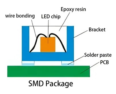
Wire bonding has been the dominant LED packaging method since the early days of the industry. In this design, a thin gold or copper wire connects the top electrode of the LED chip to the substrate.
Wire-bonding remains common in standard SMD LEDs, but as display pixels shrink, its disadvantages become increasingly evident.
As LED displays moved toward finer pixel pitches and higher brightness, flip-chip technology emerged as the next evolutionary step.
In flip-chip packaging, the LED chip is flipped upside down and mounted directly onto the substrate with solder bumps, eliminating bonding wires entirely.
Flip-chip LEDs support mass transfer and COB (Chip-on-Board) assembly — both essential for fine-pitch LED displays, where thousands of LED dies are mounted with micron-level precision.
Nevertheless, flip-chip is rapidly becoming the mainstream direction for high-end LED displays and automotive lighting.
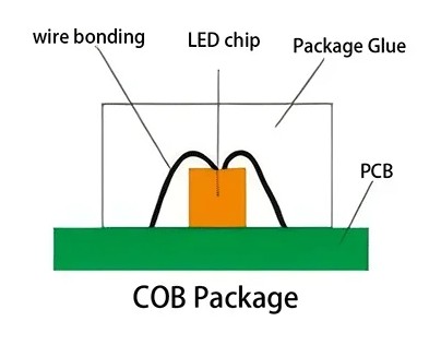
After flip-chip, the next major innovation is COB (Chip on Board) and Integrated Packaging.
In COB LEDs, multiple chips are directly mounted on a single substrate, then encapsulated with a uniform phosphor or resin layer.
Advantages:
The combination of Flip-Chip + COB is becoming the leading architecture for next-generation LED display manufacturing — offering both optical precision and mechanical durability.
| Feature | Wire-Bonding | Flip-Chip | COB / Integrated |
| Electrical Connection | Wires | Solder bumps | Direct on board |
| Heat Dissipation | Moderate | Excellent | Excellent |
| Brightness | Good | Higher | High |
| Miniaturization | Limited | Excellent | Excellent |
| Reliability | Medium | High | Very High |
| Cost | Low | Medium–High | High |
| Ideal Application | SMD displays, lighting | Fine-pitch, MicroLED | Premium displays, control rooms |
As LED displays move toward higher resolution, smaller pixels, and larger formats, packaging technologies must keep up.
Flip-chip and COB are already leading this transition, and as costs continue to fall, these technologies will become the standard choice for high-performance LED applications.
From wire bonding to flip-chip and beyond, LED packaging technology continues to evolve in pursuit of better performance, smaller pixel pitch, and longer reliability.
For LED display manufacturers and integrators, understanding these differences isn’t just technical knowledge — it’s a strategic advantage. Choosing the right packaging technology determines your display’s brightness, stability, and competitiveness in the global market.
If you’re exploring new LED solutions for fine-pitch or outdoor applications, consider partnering with a supplier experienced in flip-chip and COB packaging technologies — it’s the foundation for the next generation of LED displays.