


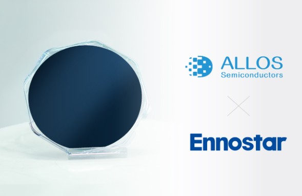
As MicroLED technology moves closer to large-scale commercialization, the industry is facing a growing demand for highly uniform, defect-controlled, and fab-compatible LED epiwafer solutions. In response to this shift, Germany-based ALLOS Semiconductors and Taiwan’s Ennostar Corporation have announced a strategic partnership aimed at bringing 200 mm GaN-on-Si LED epiwafers into volume production.
This collaboration marks a significant step toward building a silicon-compatible supply chain for MicroLED manufacturing, enabling higher yields, lower costs, and greater scalability.
One of the main barriers to MicroLED mass adoption has been the difficulty of producing high-quality epitaxial wafers at scale. Uniformity, low defect density, and consistency across wafers are critical for pixel-level applications, where even minor variations can impact performance.
ALLOS has developed a strong reputation for its GaN-on-Si epitaxy platform, engineered specifically for demanding MicroLED requirements. By partnering with Ennostar, ALLOS gains access to one of the world’s most extensive LED manufacturing infrastructures, making it possible to transition from niche production to true volume supply.
Under the agreement, Ennostar will serve as ALLOS’ manufacturing partner for 200 mm LED epiwafers. In addition to production capacity, Ennostar will contribute its advanced LED layer technologies, further enhancing device performance, brightness, and energy efficiency.
Traditional GaN-on-sapphire solutions have long dominated the LED industry, but they face limitations when it comes to integration with standard semiconductor processes. GaN-on-Si LED epiwafers offer a different path—one that aligns with the well-established silicon foundry ecosystem.
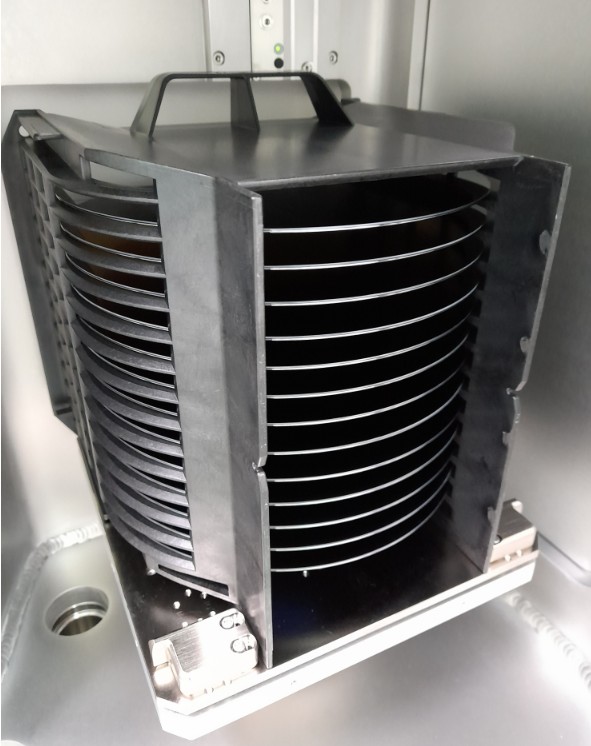
ALLOS’ epiwafers are engineered to meet silicon industry standards for cleanliness, contamination control, and thickness uniformity. With a standard 725 µm thickness, these wafers can be processed using conventional silicon fab tools, opening new opportunities for hybrid semiconductor and MicroLED manufacturing.
This compatibility is not just a technical detail—it is a strategic enabler. It allows MicroLED production to tap into the same infrastructure that has driven decades of cost reduction and yield improvement in the semiconductor industry.
By combining ALLOS’ proprietary buffer layers and n-GaN structures with Ennostar’s high-end LED layer technologies, the resulting LED epiwafers achieve brightness and energy efficiency levels comparable to traditional GaN-on-sapphire solutions.
At the same time, the GaN-on-Si platform delivers superior wafer-level uniformity and reduced micro-defect density—both essential for MicroLED arrays that may contain millions of individual emitters.
This balance of performance and manufacturability makes the new epiwafers particularly attractive for display makers seeking to scale production without sacrificing quality.
While the current focus is on 200 mm wafers, the partnership also lays the groundwork for future 300 mm LED epiwafer development. Moving to 300 mm would align MicroLED manufacturing even more closely with advanced logic and memory fabs.
Such integration could unlock new use cases beyond displays, including optical interconnects for AI processors, high-speed data communication, and energy-efficient photonic systems powered by MicroLED light sources.
ALLOS has already demonstrated 300 mm GaN-on-Si capability and continues to refine the technology with lead customers—suggesting that the transition to larger wafer formats is not a question of “if,” but “when.”
As the MicroLED industry matures, competition is increasingly shifting upstream—away from just chip design and mass transfer, and toward the foundational materials and processes that define manufacturability.
In this context, LED epiwafers are becoming a decisive factor. High uniformity, silicon fab compatibility, and scalable production are no longer optional—they are prerequisites for commercial success.
The partnership between ALLOS and Ennostar signals a clear direction for the industry: MicroLED’s future will be built on semiconductor-style manufacturing principles, with epiwafers serving as the cornerstone.